 |
||||||||||||||||||||||||||||||||||||||||||||||||||||||||||||
|
||||||||||||||||||||||||||||||||||||||||||||||||||||||||||||
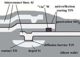
Electromigration is generally considered to be the result of momentum transfer from the electrons, which move in the applied electric field, to the ions which make up the lattice of the interconnect material. Modern semiconducting chips include a dense array of narrow, thin-film metallic conductors that serve to transport current between the various devises on the chip. These metallic conductors are called interconnects. As integrated circuits become progressively more complex, the individual components must become increasingly more reliable if the reliability of the whole is to be acceptable. However, due to continuing miniaturization of very large scale integrated (VLSI) circuits, thin-film metallic conductors or interconnects are subject to increasingly high current densities. Under these conditions, electromigration can lead to the electrical failure of interconnects in relatively short times, reducing the circuit lifetime to an unacceptable level . It is therefore of great technological importance to understand and control electromigration failure in thin film interconnects.
In conventional metal wires like those used in house wiring, joule heating limits the allowable current to about 104 A.cm-2. At current densities higher than this the wire will heat up and fuse. Because they are deposited onto large efficient single crystal silicon heat sinks, thin film interconnects in integrated circuits can sustain current densities up to 1010 A.cm-2 without immediate damage.
Electromigration causes several different kinds of failure in narrow interconnect. The most familiar are void failures along the length of the line (called internal failures) and diffusive displacements at the terminals of the line that destroy electrical contact. Recent research has shown that both of these failure modes are strongly affected by the microstructure of the line and can, therefore be delayed or overcome by metallurgical changes that alter the microstructure. Electromigration is generally considered to be the result of momentum transfer from the electrons, which move in the applied electric field, to the ions which make up the lattice of the interconnect material. For electromigration we need a lot of electrons, and also we need electron scattering Electromigration does not occur in semiconductors, but may in some semiconductor materials if they are so heavily doped that they exhibit metallic conduction. DRIVING FORCES
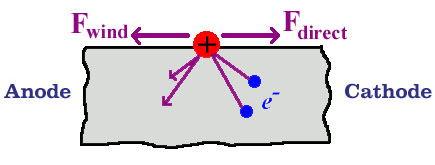
Ftotal =Fdirect+ Fwind = Z*eE For simplicity, the term “electron wind force” often refers to the net effect of these two electrical forces. This simplification will also be used throughout the following discussion. The schematic picture of these forces can be seen in figure 2.
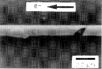
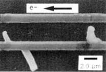
FAILURE MECHANISMS The three predominant mechanism in electromigration failure process discussed here include those associated with (a) the metallurgical-statistical properties of the interconnect, (b) the thermal accelerating process, and (c) the healing effects. The metallurgical-statistical properties of a conductor film refer to the microstructure parameters of the conductor material such as the grain size distribution, the distribution of grain boundary misorientation angles, and the inclinations of grain boundaries with respect to electron flow. These metallurgical parameters can only be dealt with statistically because they usually appear to be random. The variation of all these microstructural parameters over a film causes a non-uniform distribution of atomic flow rate. Therefore non-zero atomic flux divergence exists at the places where the number of atoms flowing into the area is not equal to the number of atoms flowing out of that area per unit time. With the non-zero atomic flux divergence, there will be either a mass depletion (divergence > 0) or accumulation (divergence <0), leading to formation of voids and hillocks. Failure results either from voids growing over the entire line width that cause breaking of the line or extrusions that cause short circuits to neighboring lines. These failure modes can be seen in figure 3.
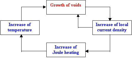
The thermal accelerating process refers to the acceleration process of electromigration damage due to the local increase in temperature. A uniform temperature distribution along an interconnect is possible only before any electromigration damage occurs. Once a void is initiated, it causes the current density to increase in the vicinity around itself because it reduces the cross sectional area of the conductor.
The increase of the local current density is referred as the current crowding. Since joule heating is proportional to the square of current density, the current crowding effect leads to a local temperature rise around the void that in turn further accelerates the void growth. The whole process continues till the void is large enough to break the line. Such a process can be seen in figure 4.
The healing effects refer to those caused by the atomic flow in the direction opposite to the electron wind force, the back-flow, during or after electromigration. This back-flow of mass begins to take place once a redistribution of mass has begun to form. It tends to reduce the failure rate during electromigration and partially heals the damage after current is removed. The cause of this back-flow of mass is the inhomogenities, such as temperature and/or concentration gradients, resulting from electromigration damage. |
||||||||||||||||||||||||||||||||||||||||||||||||||||||||||||