 |
||||||||||||||||||||||
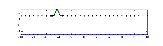
Electromigration Induced Edge Void Dynamics on the Interconnect Surface The morphology of an initially perfectly flat surface having a perturbation in the shape of Gaussian edge-void is demonstrated in Figure., where the positive direction of electric field is from the left (anode) to the right (cathode). The scaled interconnect width is denoted as w and the void depth and the specimen length are given by a and L , respectively. These are all scaled with respect to the arbitrary length denoted by lo . Three different crystal planes in a FCC structure, {110}, {100}and {111} are considered, which may be charactered by two, four and six fold symmetry axises, respectively.
|
||||||||||||||||||||||